1. Crystal Structure and Polytypism of Silicon Carbide
1.1 Cubic and Hexagonal Polytypes: From 3C to 6H and Beyond
(Silicon Carbide Ceramics)
Silicon carbide (SiC) is a covalently adhered ceramic made up of silicon and carbon atoms arranged in a tetrahedral sychronisation, creating one of the most complex systems of polytypism in materials science.
Unlike the majority of porcelains with a single secure crystal structure, SiC exists in over 250 recognized polytypes– distinctive stacking series of close-packed Si-C bilayers along the c-axis– varying from cubic 3C-SiC (also called β-SiC) to hexagonal 6H-SiC and rhombohedral 15R-SiC.
The most usual polytypes used in design applications are 3C (cubic), 4H, and 6H (both hexagonal), each showing a little various digital band frameworks and thermal conductivities.
3C-SiC, with its zinc blende structure, has the narrowest bandgap (~ 2.3 eV) and is generally grown on silicon substrates for semiconductor devices, while 4H-SiC offers remarkable electron mobility and is chosen for high-power electronic devices.
The solid covalent bonding and directional nature of the Si– C bond confer phenomenal solidity, thermal security, and resistance to slip and chemical attack, making SiC perfect for severe environment applications.
1.2 Problems, Doping, and Digital Properties
Despite its architectural complexity, SiC can be doped to attain both n-type and p-type conductivity, allowing its use in semiconductor devices.
Nitrogen and phosphorus act as donor contaminations, presenting electrons right into the conduction band, while light weight aluminum and boron function as acceptors, creating holes in the valence band.
However, p-type doping effectiveness is limited by high activation energies, particularly in 4H-SiC, which presents difficulties for bipolar device style.
Native issues such as screw misplacements, micropipes, and stacking faults can break down tool performance by working as recombination facilities or leak courses, requiring top quality single-crystal development for electronic applications.
The vast bandgap (2.3– 3.3 eV depending upon polytype), high break down electrical area (~ 3 MV/cm), and outstanding thermal conductivity (~ 3– 4 W/m · K for 4H-SiC) make SiC much superior to silicon in high-temperature, high-voltage, and high-frequency power electronic devices.
2. Processing and Microstructural Design
( Silicon Carbide Ceramics)
2.1 Sintering and Densification Strategies
Silicon carbide is inherently challenging to densify as a result of its solid covalent bonding and reduced self-diffusion coefficients, calling for innovative processing techniques to accomplish complete density without ingredients or with very little sintering help.
Pressureless sintering of submicron SiC powders is feasible with the addition of boron and carbon, which promote densification by eliminating oxide layers and boosting solid-state diffusion.
Hot pressing applies uniaxial stress during home heating, allowing full densification at reduced temperature levels (~ 1800– 2000 ° C )and creating fine-grained, high-strength components appropriate for reducing devices and put on components.
For large or intricate forms, reaction bonding is used, where permeable carbon preforms are infiltrated with molten silicon at ~ 1600 ° C, developing β-SiC sitting with minimal shrinking.
Nonetheless, recurring free silicon (~ 5– 10%) stays in the microstructure, limiting high-temperature performance and oxidation resistance over 1300 ° C.
2.2 Additive Manufacturing and Near-Net-Shape Construction
Recent breakthroughs in additive manufacturing (AM), specifically binder jetting and stereolithography making use of SiC powders or preceramic polymers, enable the construction of intricate geometries formerly unattainable with standard methods.
In polymer-derived ceramic (PDC) routes, liquid SiC forerunners are shaped using 3D printing and afterwards pyrolyzed at high temperatures to yield amorphous or nanocrystalline SiC, usually needing additional densification.
These methods reduce machining costs and material waste, making SiC more accessible for aerospace, nuclear, and warm exchanger applications where complex designs improve performance.
Post-processing steps such as chemical vapor infiltration (CVI) or liquid silicon seepage (LSI) are sometimes used to boost density and mechanical integrity.
3. Mechanical, Thermal, and Environmental Efficiency
3.1 Toughness, Solidity, and Wear Resistance
Silicon carbide rates amongst the hardest well-known materials, with a Mohs hardness of ~ 9.5 and Vickers solidity surpassing 25 GPa, making it highly resistant to abrasion, erosion, and damaging.
Its flexural toughness typically ranges from 300 to 600 MPa, relying on processing technique and grain size, and it retains toughness at temperature levels up to 1400 ° C in inert environments.
Fracture toughness, while moderate (~ 3– 4 MPa · m ¹/ TWO), is sufficient for lots of architectural applications, especially when integrated with fiber support in ceramic matrix compounds (CMCs).
SiC-based CMCs are used in wind turbine blades, combustor liners, and brake systems, where they use weight financial savings, fuel efficiency, and prolonged service life over metal counterparts.
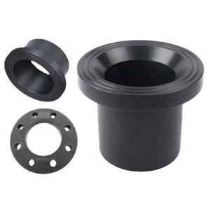
Its superb wear resistance makes SiC ideal for seals, bearings, pump elements, and ballistic shield, where resilience under severe mechanical loading is critical.
3.2 Thermal Conductivity and Oxidation Stability
Among SiC’s most useful buildings is its high thermal conductivity– as much as 490 W/m · K for single-crystal 4H-SiC and ~ 30– 120 W/m · K for polycrystalline kinds– surpassing that of several metals and enabling efficient warmth dissipation.
This home is vital in power electronics, where SiC tools produce less waste warmth and can run at greater power densities than silicon-based gadgets.
At raised temperatures in oxidizing environments, SiC creates a protective silica (SiO TWO) layer that slows down additional oxidation, giving great environmental sturdiness up to ~ 1600 ° C.
However, in water vapor-rich atmospheres, this layer can volatilize as Si(OH)FOUR, bring about accelerated degradation– a vital obstacle in gas wind turbine applications.
4. Advanced Applications in Energy, Electronic Devices, and Aerospace
4.1 Power Electronic Devices and Semiconductor Tools
Silicon carbide has transformed power electronic devices by enabling devices such as Schottky diodes, MOSFETs, and JFETs that operate at greater voltages, frequencies, and temperatures than silicon matchings.
These tools reduce power losses in electric cars, renewable resource inverters, and commercial electric motor drives, adding to global energy performance renovations.
The ability to run at junction temperatures over 200 ° C enables streamlined air conditioning systems and raised system reliability.
Additionally, SiC wafers are used as substratums for gallium nitride (GaN) epitaxy in high-electron-mobility transistors (HEMTs), combining the benefits of both wide-bandgap semiconductors.
4.2 Nuclear, Aerospace, and Optical Equipments
In atomic power plants, SiC is a key element of accident-tolerant fuel cladding, where its reduced neutron absorption cross-section, radiation resistance, and high-temperature stamina enhance safety and security and performance.
In aerospace, SiC fiber-reinforced compounds are made use of in jet engines and hypersonic automobiles for their lightweight and thermal security.
Furthermore, ultra-smooth SiC mirrors are employed in space telescopes because of their high stiffness-to-density ratio, thermal security, and polishability to sub-nanometer roughness.
In summary, silicon carbide porcelains represent a cornerstone of modern innovative materials, incorporating remarkable mechanical, thermal, and electronic residential properties.
With precise control of polytype, microstructure, and handling, SiC continues to enable technical advancements in energy, transport, and severe environment design.
5. Supplier
TRUNNANO is a supplier of Spherical Tungsten Powder with over 12 years of experience in nano-building energy conservation and nanotechnology development. It accepts payment via Credit Card, T/T, West Union and Paypal. Trunnano will ship the goods to customers overseas through FedEx, DHL, by air, or by sea. If you want to know more about Spherical Tungsten Powder, please feel free to contact us and send an inquiry(sales5@nanotrun.com).
Tags: silicon carbide ceramic,silicon carbide ceramic products, industry ceramic
All articles and pictures are from the Internet. If there are any copyright issues, please contact us in time to delete.
Inquiry us