1. Product Fundamentals and Architectural Characteristics of Alumina Ceramics
1.1 Crystallographic and Compositional Basis of α-Alumina
(Alumina Ceramic Substrates)
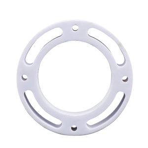
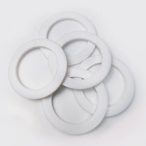
Alumina ceramic substratums, mainly made up of aluminum oxide (Al two O SIX), work as the backbone of modern digital packaging due to their outstanding balance of electrical insulation, thermal security, mechanical strength, and manufacturability.
The most thermodynamically steady stage of alumina at heats is diamond, or α-Al Two O SIX, which crystallizes in a hexagonal close-packed oxygen latticework with light weight aluminum ions inhabiting two-thirds of the octahedral interstitial websites.
This dense atomic plan imparts high hardness (Mohs 9), outstanding wear resistance, and solid chemical inertness, making α-alumina appropriate for severe operating environments.
Business substrates usually consist of 90– 99.8% Al ₂ O FIVE, with small additions of silica (SiO TWO), magnesia (MgO), or rare planet oxides used as sintering help to advertise densification and control grain growth during high-temperature processing.
Greater purity qualities (e.g., 99.5% and over) display exceptional electric resistivity and thermal conductivity, while reduced pureness versions (90– 96%) use economical services for less demanding applications.
1.2 Microstructure and Flaw Engineering for Electronic Integrity
The efficiency of alumina substratums in electronic systems is seriously depending on microstructural harmony and issue minimization.
A fine, equiaxed grain framework– normally ranging from 1 to 10 micrometers– guarantees mechanical stability and decreases the possibility of crack proliferation under thermal or mechanical anxiety.
Porosity, particularly interconnected or surface-connected pores, must be minimized as it breaks down both mechanical strength and dielectric efficiency.
Advanced processing strategies such as tape spreading, isostatic pressing, and regulated sintering in air or regulated ambiences make it possible for the manufacturing of substrates with near-theoretical thickness (> 99.5%) and surface roughness below 0.5 µm, essential for thin-film metallization and cord bonding.
Additionally, pollutant segregation at grain limits can lead to leakage currents or electrochemical movement under predisposition, requiring stringent control over basic material purity and sintering problems to make sure lasting dependability in moist or high-voltage environments.
2. Manufacturing Processes and Substrate Fabrication Technologies
( Alumina Ceramic Substrates)
2.1 Tape Spreading and Environment-friendly Body Processing
The manufacturing of alumina ceramic substratums begins with the preparation of a highly dispersed slurry containing submicron Al ₂ O three powder, natural binders, plasticizers, dispersants, and solvents.
This slurry is refined by means of tape spreading– a continual technique where the suspension is spread over a relocating carrier film utilizing a precision physician blade to accomplish uniform density, commonly between 0.1 mm and 1.0 mm.
After solvent evaporation, the resulting “environment-friendly tape” is flexible and can be punched, pierced, or laser-cut to create using holes for vertical affiliations.
Multiple layers may be laminated flooring to develop multilayer substrates for complicated circuit combination, although the majority of commercial applications use single-layer setups as a result of cost and thermal development considerations.
The environment-friendly tapes are after that very carefully debound to remove organic additives through managed thermal disintegration before final sintering.
2.2 Sintering and Metallization for Circuit Combination
Sintering is performed in air at temperatures in between 1550 ° C and 1650 ° C, where solid-state diffusion drives pore elimination and grain coarsening to accomplish full densification.
The direct contraction during sintering– typically 15– 20%– should be precisely predicted and made up for in the design of green tapes to ensure dimensional precision of the final substrate.
Following sintering, metallization is applied to develop conductive traces, pads, and vias.
Two key methods dominate: thick-film printing and thin-film deposition.
In thick-film modern technology, pastes consisting of steel powders (e.g., tungsten, molybdenum, or silver-palladium alloys) are screen-printed onto the substratum and co-fired in a decreasing atmosphere to create robust, high-adhesion conductors.
For high-density or high-frequency applications, thin-film processes such as sputtering or dissipation are made use of to down payment attachment layers (e.g., titanium or chromium) adhered to by copper or gold, allowing sub-micron patterning via photolithography.
Vias are full of conductive pastes and discharged to develop electric interconnections between layers in multilayer styles.
3. Functional Characteristics and Performance Metrics in Electronic Solution
3.1 Thermal and Electrical Actions Under Functional Tension
Alumina substratums are valued for their positive combination of moderate thermal conductivity (20– 35 W/m · K for 96– 99.8% Al ₂ O SIX), which makes it possible for effective warmth dissipation from power tools, and high volume resistivity (> 10 ¹⁴ Ω · cm), making certain minimal leakage current.
Their dielectric continuous (εᵣ ≈ 9– 10 at 1 MHz) is secure over a wide temperature and regularity range, making them ideal for high-frequency circuits up to a number of gigahertz, although lower-κ materials like light weight aluminum nitride are liked for mm-wave applications.
The coefficient of thermal growth (CTE) of alumina (~ 6.8– 7.2 ppm/K) is fairly well-matched to that of silicon (~ 3 ppm/K) and specific product packaging alloys, minimizing thermo-mechanical stress throughout tool procedure and thermal cycling.
Nonetheless, the CTE inequality with silicon continues to be a problem in flip-chip and direct die-attach setups, often requiring compliant interposers or underfill products to mitigate tiredness failing.
3.2 Mechanical Toughness and Environmental Toughness
Mechanically, alumina substrates exhibit high flexural stamina (300– 400 MPa) and superb dimensional security under lots, enabling their use in ruggedized electronic devices for aerospace, automotive, and industrial control systems.
They are immune to vibration, shock, and creep at elevated temperatures, maintaining structural honesty up to 1500 ° C in inert environments.
In moist atmospheres, high-purity alumina reveals very little dampness absorption and superb resistance to ion migration, making certain lasting reliability in outdoor and high-humidity applications.
Surface area firmness likewise secures against mechanical damages during handling and assembly, although care has to be taken to avoid edge chipping because of fundamental brittleness.
4. Industrial Applications and Technical Effect Throughout Sectors
4.1 Power Electronics, RF Modules, and Automotive Solutions
Alumina ceramic substratums are common in power electronic modules, including insulated entrance bipolar transistors (IGBTs), MOSFETs, and rectifiers, where they offer electrical isolation while assisting in heat transfer to heat sinks.
In superhigh frequency (RF) and microwave circuits, they act as carrier platforms for hybrid integrated circuits (HICs), surface area acoustic wave (SAW) filters, and antenna feed networks due to their steady dielectric residential or commercial properties and low loss tangent.
In the automotive industry, alumina substrates are made use of in engine control units (ECUs), sensor bundles, and electrical car (EV) power converters, where they sustain heats, thermal cycling, and exposure to corrosive fluids.
Their reliability under extreme problems makes them important for safety-critical systems such as anti-lock stopping (ABDOMINAL MUSCLE) and advanced vehicle driver support systems (ADAS).
4.2 Clinical Tools, Aerospace, and Arising Micro-Electro-Mechanical Solutions
Beyond consumer and industrial electronics, alumina substratums are used in implantable medical tools such as pacemakers and neurostimulators, where hermetic sealing and biocompatibility are vital.
In aerospace and defense, they are made use of in avionics, radar systems, and satellite interaction components as a result of their radiation resistance and stability in vacuum cleaner environments.
In addition, alumina is progressively used as a structural and shielding platform in micro-electro-mechanical systems (MEMS), including stress sensing units, accelerometers, and microfluidic devices, where its chemical inertness and compatibility with thin-film handling are useful.
As electronic systems continue to require higher power thickness, miniaturization, and dependability under extreme problems, alumina ceramic substratums stay a cornerstone material, connecting the gap in between performance, cost, and manufacturability in sophisticated electronic packaging.
5. Provider
Alumina Technology Co., Ltd focus on the research and development, production and sales of aluminum oxide powder, aluminum oxide products, aluminum oxide crucible, etc., serving the electronics, ceramics, chemical and other industries. Since its establishment in 2005, the company has been committed to providing customers with the best products and services. If you are looking for high quality 99 alumina, please feel free to contact us. (nanotrun@yahoo.com)
Tags: Alumina Ceramic Substrates, Alumina Ceramics, alumina
All articles and pictures are from the Internet. If there are any copyright issues, please contact us in time to delete.
Inquiry us